IC Testing and Characterization
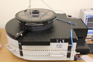
The INOVYS Ocelot-ZFP Automatic Testing Equipment (ATE) provides testing capability on integrated circuits (IC). With its 512 data channels, each of which can read and send data at a speed of up to 50 MHz frequency, it is an industrial grade equipment rated fit for manufacture test on state-of-art level of integration. It is capable of performing analog test, parametric measurements, digital communications with on-chip design-for-test (DFT) circuitry, and speed tests with functional and path-delay-fault (PDF) patterns. Within the purview of our research interests, it allows us to design and test digital and analog hardware attacks and cybersecurity countermeasures, as well as to conduct electrical experiment tests on potential counterfeit ICs.
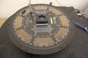
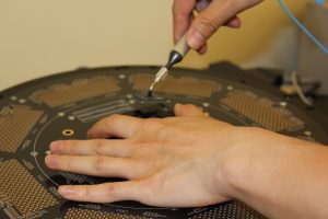
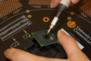
In the past, we have designed and fabricated a dedicated load board and an ancillary socket to mount a commercial IC for test. Fabricated at 55 nm technology, the IC under test was one of the most cutting edge products among its peers. In addition to dedicated load boards and sockets, it is also possible to design one that serves general purposes and is fit for use with ICs in any package at reduced timing performance.
NanoProber
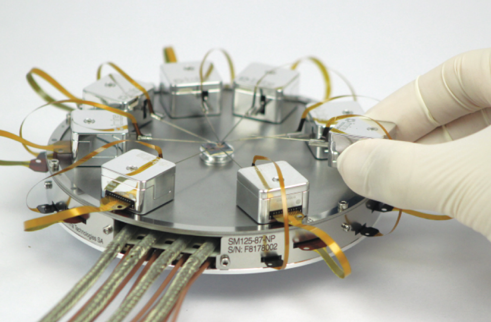
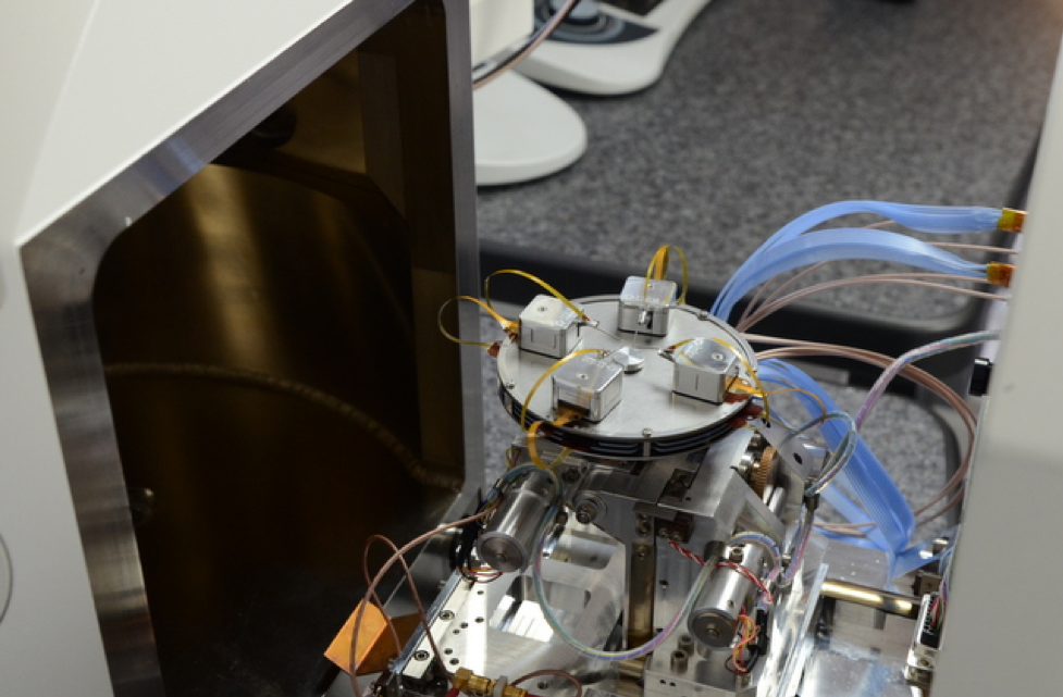
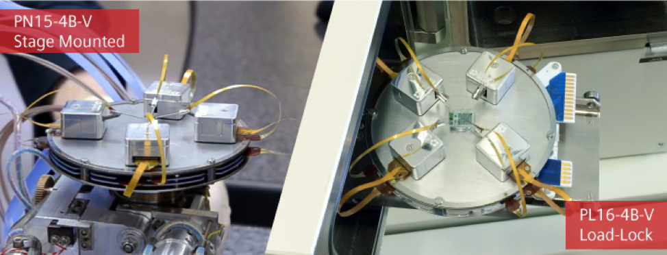
Imina Technologies’ Nanoprobing SEM Solutions are turnkey for electrical characterization of microelectronic devices and in situ semiconductor failure analysis. Up to 8 miBot™ nanoprobers can be delivered in various configurations to adapt to customer applications requirements and equipment. The miBOT is famously easy-to-use and versatile piezo actuated micro robots that allows you to position the probes over millimeter scale samples with a resolution down to the nanometer. The 4 degrees of freedom of these nanoprobers enables the operator to easily adjust the orientation of probes in situ during experiment.
Specifically designed for low current measurements, electrical characterization of nanostructures can be carried out with third party source-meter units (SMU) and signal analyzers through the shielded cabling, featuring an excellent signal-to-noise ratio.
Equipped with the EBIC/EBAC, in situ preamplifiers and scan generators are compatible with the Nanoprobing Solutions to perform quantitative EBIC and low noise EBAC/RCI analyses as well.
PHEMOS-1000
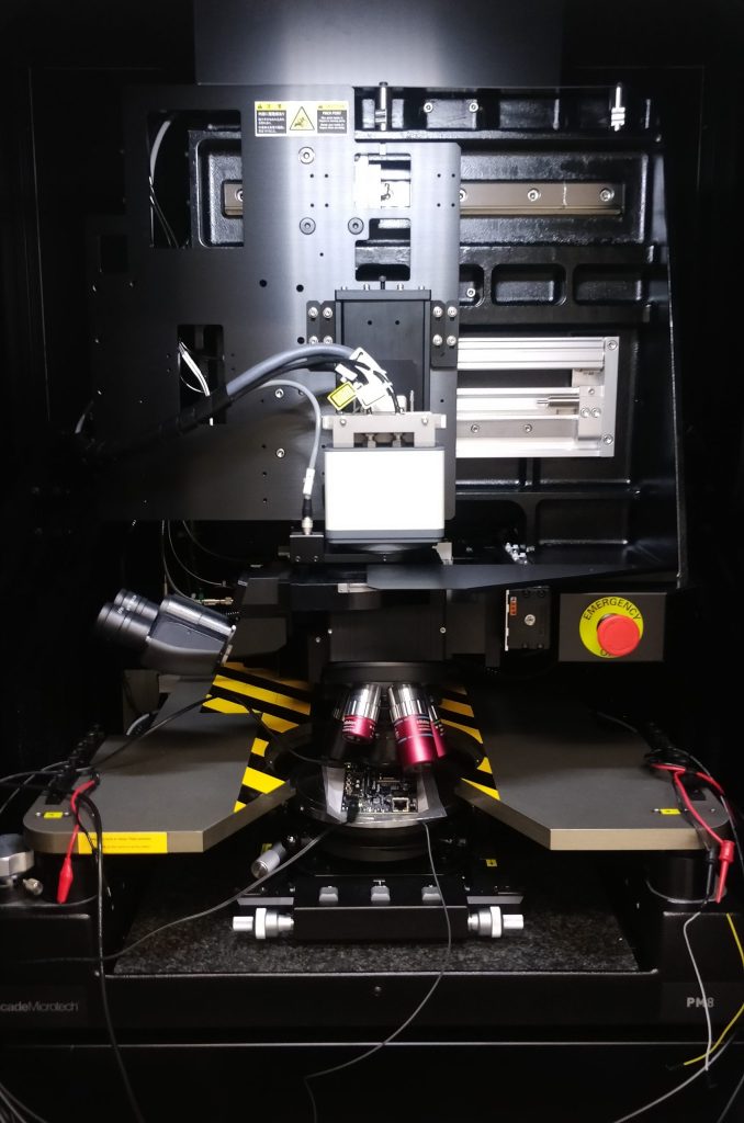
The PHEMOS-1000 is a high-resolution optical emission microscope in near infrared (NIR) spectrum that localizes failures in semiconductor devices by detecting the light emissions caused by semiconductor device defects. Moreover, its laser scan system allows acquiring high-resolution pattern images. Different types of detectors are available for various analysis techniques, such as photon emission analysis (PEM), electro-optical probing (EOP), and OBIRCH analysis. In addition to failure analysis applications, this microscope can be deployed for reverse-engineering of integrated circuits (ICs) from the backside of the package.

