Nanoscale Imaging
Nanoscale imaging research, which includes x-ray, scanning electron microscopy (SEM), and light microscopy, in the FICS Research SCAN Lab is supported by three state-of-the-art, stand-alone systems which were installed in the summer of 2016 through a
recent partnership between UF and TESCAN, a leading manufacturer in electron microscopy.
The new Skyscan 2211 system which enables non-destructive 3D X-ray computed tomography on micron and nano level resolution. 3D tomography can reveal internal structure information of objects such as Printed Circuit boards and microchips with imaging resolution down to few hundreds of nano meters. FICS Research faculty are already developing techniques based on X-ray tomography to do fast and easy PCB reverse engineering, which is currently a very important copyright and security topic for industry and government entities.
Two dual beam systems, the FERA and LYRA, which enable unique nano level imaging and milling capabilities. LYRA is a dual beam system with Gallium Focused Ion Beam (FIB) and Electron Beam columns. The GaFIB can be used for fine milling on many types of samples in a specific range of time. FERA is a Xe-Plasma Focued Ion Beam (FIB) with Electron Beam column. Plasma ion source can reach up to 2µA for the probe current and enables milling rates of up to 50-60 times faster than a regular FIB system. Reverse engineering, failure localization, sample prep for micro or nano probing, etc. are some of the capabilities that will be enabled by these systems. In addition the open source format of the controlling systems on these microscopes provides a platform for computational microscopy where regular microscopy can be changed to intelligent microscopy based on the images and pre-knowledge of the sample.
Equipment Details:
Leica DVM6
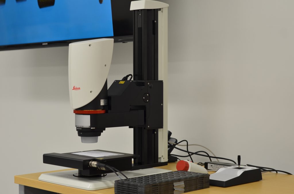
The Leica DVM6 is a high resolution digital microscope with 16:1 zoom ratio. DVM6 has a fully apochromatic corrected optics and a 10M pixel camera with fast live imaging mode. The motorized stage has 3 degrees of freedom in x, y, and z direction which enables automatic stitching and 3D surface imaging. In addition, with the Mark and Find software available on this system, user can define multiple stage locations and revisit them automatically during experiment setup or as part of time-lapse experiment. Such capabilities are very beneficial for a variety of hardware security projects including integrated circuits counterfeit detection, PCB reverse engineering, wafers failure analysis, etc.
SKYSCAN 2211 MultiScale X-ray Nano-CT System
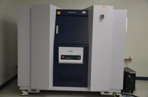
The X-ray Nano-CT system covers the largest range of objects sizes and spatial resolution available in one instrument. The system has capacity for scanning and 3D non-destructive reconstruction of internal micro-structures on object sizes > 8inches (200mm, such as PCBs) as well as sub-micron resolution for small samples (such as microchips). It is an ‘open-type’ (pumped) X-ray source, 20-190Kv with standard Be window, with sub-micron spot size and two X-ray detectors: flat panel for large objects and 11Mpixel cooled CCD for scanning with the highest resolution down to 100 nm. It automatically adjusts for variable acquisition geometry and phase-contrast enhancements allows the best possible quality in relatively short scanning times.
FERA-3 GMH Xe-Plasma FIB with Integrated Schottky FESEM
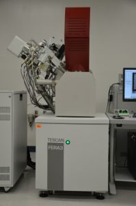
The FERA-3 is a fully PC controlled Scanning Electron Microscope (SEM) with Schottky field emission cathode in combination with Xe Plasma Focused Ion Beam (i-FIB) column. This dual beam is also equipped with Gas Injection System (GIS) which enables depositing conductive and non-conductive material. The Ion optics is a fully integrated Xe Plasma Ion source with 2pA-2µA probe current range and 3Kv-30Kv beam energy range. This probe will enable the milling rates to be typically 50-60 times faster than a conventional Ga (Liquid Metal Ion Source) LIMIS FIB. Imaging is based on a high performance DSP-based Image Acquisition system in this microscope, which is capable of acquiring images up to 16k x 16k pixels with 16-bit dynamic range (pixel depth) and it can continuously adjust the scanning rates from 20ns per pixel to 10ms per pixel to achieve a better signal to noise ratio.
LYRA-3 XMH Ga LIMIS FIB with Integrated Schottky FESEM
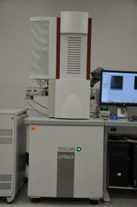
The LYRA-3 is a fully PC controlled SEM with Schottky field emission cathode in combination with a Gallium Focused Ion Beam (i-FIB) column. Wide field optics design in this system is available with an ultimate resolution of 1.2 nm. The ion column is a fully integrated Canion FIB column with Ga (Liquid Metal Ion Source) LIMIS, with 1pa-40nA probe current range, and 0.5kv-30kv beam energy, which provides better control of material depositing or milling of a fine size item. The system also has a fully integrated XYZ piezo nano-manipulator with integrated closed loop Nanoposition sensors and controllers for TEM sample preparation. The Gas Injection System is equipped with automatic nozzle positioning and automatic temperature control. Available precursors for deposition are: Carbon, Platinum, Tungsten, and Silicon Oxide plus Fluorine and water for etching.
ORION NanoFab
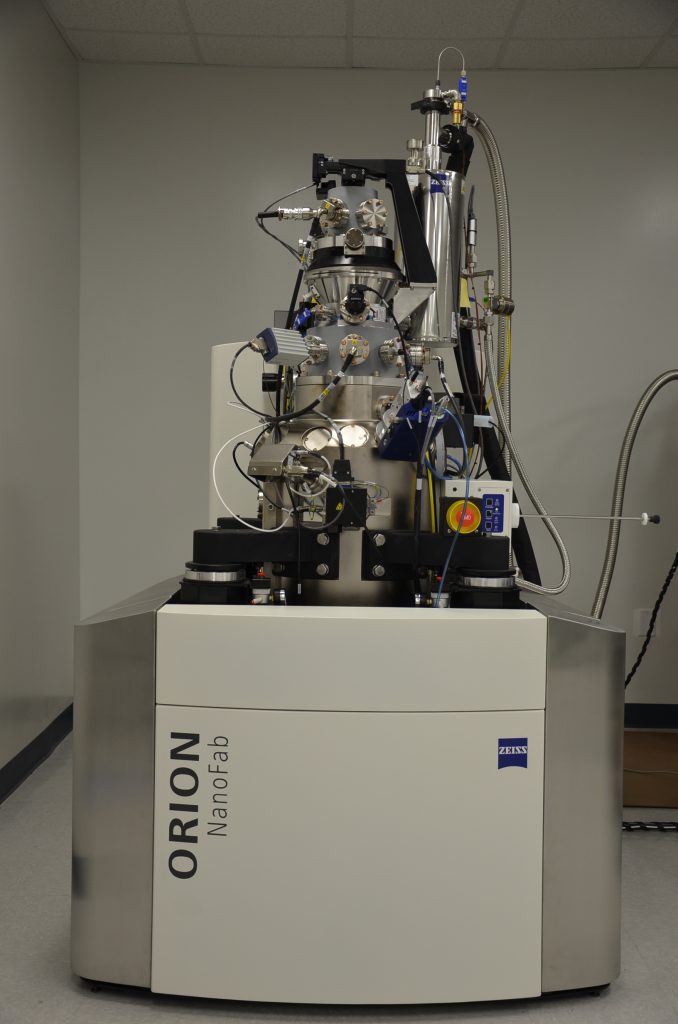
The ORION NanoFab is a multi-ion column system including Helium and Neon that provides a complete sub-10 nanometer nano-fabrication and sub-nanometer imaging solution for research in a wide range of applications. The imaging resolution with Helium ion is 0.5 nm, which is not achievable by regular Ga ion FIBs or SEMs. ORION NanoFab features the NanoPatterning and Visualization Engine – an integrated hardware and software control system. NVPE incorporates a dedicated 16 bit scan generator for each NanoFab column and dual signal acquisition hardware supporting real-time advanced patterning and visualization. It allows users to completely control the beam by a GUI and create a range of fully editable shapes including rectangles, trapezoids, polygons, lines, polylines, ellipses and spots. The next step allows these shapes can be vector filled while maintaining full control over dose variation and patterning parameters.
PHEMOS-1000
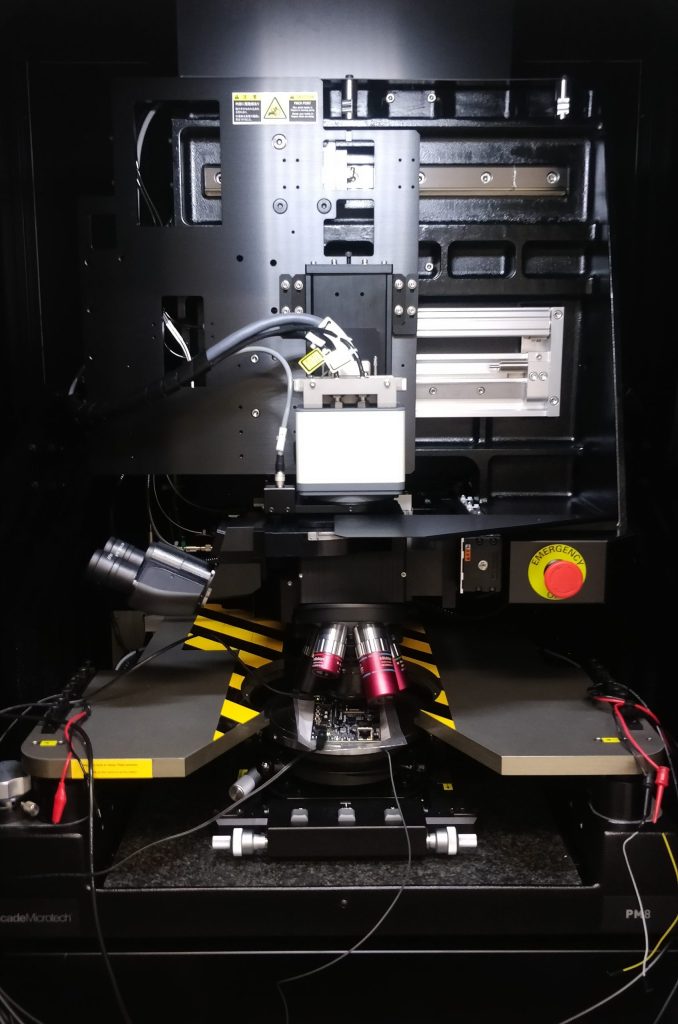
The PHEMOS-1000 is a high-resolution optical emission microscope in near infrared (NIR) spectrum that localizes failures in semiconductor devices by detecting the light emissions caused by semiconductor device defects. Moreover, its laser scan system allows acquiring high-resolution pattern images. Different types of detectors are available for various analysis techniques, such as photon emission analysis (PEM), electro-optical probing (EOP), and OBIRCH analysis. In addition to failure analysis applications, this microscope can be deployed for reverse-engineering of integrated circuits (ICs) from the backside of the package.
